Check out our free guide with common Fpga Design Engineer interview questions and tips.
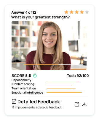
Practice with a mock video interview conducted by our virtual recruiter.
Receive a detailed performance review from experienced HR professionals.
Get personalized, strategic feedback highlighting your strengths and areas to improve.
Specific examples of your achievements and skills can demonstrate your qualifications for the role. Try to provide quantifiable examples wherever possible.
FPGA design engineers are responsible for designing, testing, and implementing FPGA-based solutions in various industries, including telecommunications, aerospace, and defense. If you are preparing for an FPGA design engineer job interview, here are the top 20 interview questions and answers to help you get the job.
FPGAs, or field-programmable gate arrays, are integrated circuits that can be programmed by the user after manufacturing to perform specific tasks. They are used in electronic devices that require high-speed processing, low power consumption, and reconfigurability.
FPGAs offer several advantages over other types of integrated circuits, including fast and efficient processing, low power consumption, and flexibility to reconfigure the chip for different applications without the need for hardware changes.
The different types of FPGA architectures include lookup table-based, antifuse-based, and flash-based. The lookup table-based architecture uses a RAM-based structure to perform logic operations, while the antifuse-based architecture uses a one-time programmable structure. The flash-based architecture uses a reprogrammable structure to allow for changes in the programming.
The key considerations when selecting an FPGA for a particular application include performance requirements, power consumption, cost, and reconfigurability.
The most commonly used programming languages for FPGA design include VHDL and Verilog.
A testbench is a module used to test the functionality of a design. It is used to simulate input and output signals that the design will encounter in the real world.
A synchronous reset is a signal that is synchronized to the clock and used to reset the state of the design. An asynchronous reset is a signal that is not synchronized to the clock and can be triggered at any time.
Combinational logic refers to logic circuits that have no memory elements and perform logical operations based on input only. Sequential logic circuits have memory elements and perform operations based on the current and previous input values.
A flip-flop is a sequential circuit element that is sensitive to clock transitions and latches data on the rising or falling edge of the clock. A latch is a circuit element that latches data continuously without the need for a clock signal.
A D flip-flop has a single data input and a clock input and latches data on each clock cycle. A JK flip-flop has two data inputs, J and K, and can be used for toggling, counting, or serial to parallel conversion.
A synchronous counter is a counter that is synchronized to the clock and produces an output on each clock cycle. An asynchronous counter is a counter that produces an output based on the state of the previous counter and does not require a clock signal.
Fan-out refers to the number of logic gates that can be driven by a single output signal. Fan-in refers to the number of input signals that can be connected to a single logic gate.
Clock skew is the difference in arrival times of a clock signal at different locations in a design. It can cause timing errors and affect the performance of the design.
Routing delay is a delay that occurs when a signal travels through the interconnects between logic gates. It can cause timing errors and affect the performance of the design.
A critical path is the longest path in a design from the input to the output. It determines the maximum operating frequency and can affect the performance of the design.
Timing constraints are used to ensure that the design meets its timing requirements. They define the maximum operating frequency, setup and hold times, and other timing parameters.
CDC, or clock domain crossing, is a situation in which signals cross over from one clock domain to another. It can lead to timing errors and requires careful handling, including clock domain synchronization, glitch filtering, and metastability protection.
Synthesis is the process of converting a high-level design specification into a gate-level netlist. Simulation is the process of testing the functionality and performance of the design using software tools or hardware.
Verification is the process of ensuring that the design meets its functional and performance requirements. It is important to prevent errors and reduce the risk of costly mistakes.
The design flow for FPGA design typically includes design entry, synthesis, simulation, place and route, and verification.
These are the top 20 FPGA design engineer interview questions and answers that will help you prepare for your job interview. Be sure to review your skills and knowledge in FPGA design to increase your chances of landing that dream job.
When it comes to nailing an interview for an FPGA Design Engineer position, preparation is key. Apart from having a solid understanding of FPGA design principles and computer architecture, there are a few things you can do to increase your chances of landing the job.
Brush up on your experience with verilog, VHDL and other programming languages commonly used in FPGA design. Be prepared to discuss your experience with various FPGA architectures, including Xilinx and Altera.
Be ready to talk about the design tools you’ve used, including Quartus, Xilinx ISE, and Vivado. Also, make sure you’re comfortable with the debugging techniques and simulation methodologies that you have experience with.
Dig into the products, services, and culture of the company you’re interviewing with. Familiarizing yourself with the organization’s mission, clients, and industry may help you prepare questions and better understand what the interviewer is seeking in a candidate.
The interviewer may ask to see examples of your prior work. Be prepared to show your portfolio and explain your design process. Have specifics prepared such as what inspired you in your design element choices, how you work around constraints or existing designs, and what goals you achieved with the project.
The interviewer may present you with hypothetical design challenges to assess your ability to troubleshoot complex problems. This often involves designing an FPGA solution for a given problem from scratch. You can prepare for these types of questions by practicing design challenges and answering prompts under a timed test.
Remember, the interview is an opportunity for you to show your potential employer why you’re the best candidate for the job. Be confident in your abilities, speak naturally, and come prepared with questions of your own. This is your chance to show how passionate and driven you are, so make the most of it.
By preparing for an FPGA design engineer interview, you’ll increase your chances of landing the job. Review your fundamentals, familiarize yourself with design tools, research the company, show examples of your work, prepare to answer hypothetical questions and be confident, and natural in the interview.
While it's important to demonstrate your knowledge, overusing industry jargon can confuse your interviewer or make it seem like you're trying too hard. Aim to communicate clearly and effectively.
 Professional
 Simple
 Modern
 Creative
 Premium
 Popular